A2 amp driver PCB
(Photos are hyperlinked to higher resolution images - just click on them).
This is a driver PCB for a class A2 amp. I designed it for single ended use, but you could also use two of them with an input transformer for a push-pull amp.
I designed it for use in a SE amp using the rare 4304CB / VT-62 / or 834 triode. It can be used in many different applications, even in class A1 use, though it is optimized to drive grid current, and for use with loop NFB.
The circuit uses a single 2-section tube that has a triode and pentode. Specially, a high mu triode (like 12AX7 or 12AT7) plus a high gm pentode (intended for video output use). It uses a tube with a 9DX base. At a minimum, that includes the following tubes:
| Tube | Triode Mu | Pentode gm |
| 6JT8 | 100 | 20k |
| 6LY8 | 100 | 20k |
| 6KV8 | 70 | 21k |
| 6KR8 | 46 | 20k |
| 6LQ8 | 46 | 21k |
| 6LB8 | 30 | 20k |
| 6HZ8 | 70 | 12.6k |
Most of these tubes are in standard noval envelope, but some are "fat boy" noval types. Here is a 6LY8 (left) and 6JT8 tube:
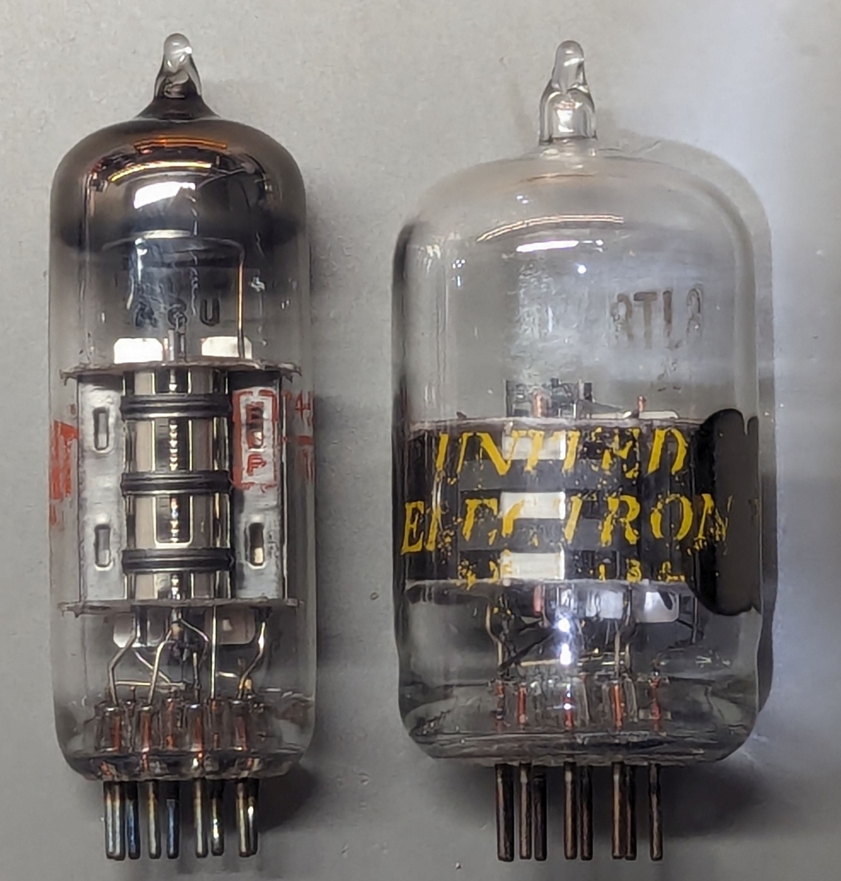
These tubes were used in later tubed black-and-white TV sets and seem to be plentiful. At least as of now, these tubes are not popular among audio types, so they are very affordable - most I bought were $3 each or less. I hope they say that way.
To allow as much NFB as possible with a single stage, I chose the 6LY8 for the VT-62 amp. The 6JT8 was very similar.
The circuit uses the triode as a standard amplifier using cathode boas and a cascode CCS plate load. This stage is cap coupled to the pentode, which is connected as a triode mode cathode follower, with a CCS cathode load. The cathode directly connects to the power tube grid.
To get an output that is typically centered close to 0 volts, both a positive and negative supply voltage are needed. I designed this for +250V and -100V. You can vary this based on your output needs, but keep in mind reducing the positive voltage will limit your output swing. The negative supply needs to be at least whatever your negative output swing needs to be, plus maybe 10 volts for CCS headroom.
Here is the schematic (or download a PDF file):
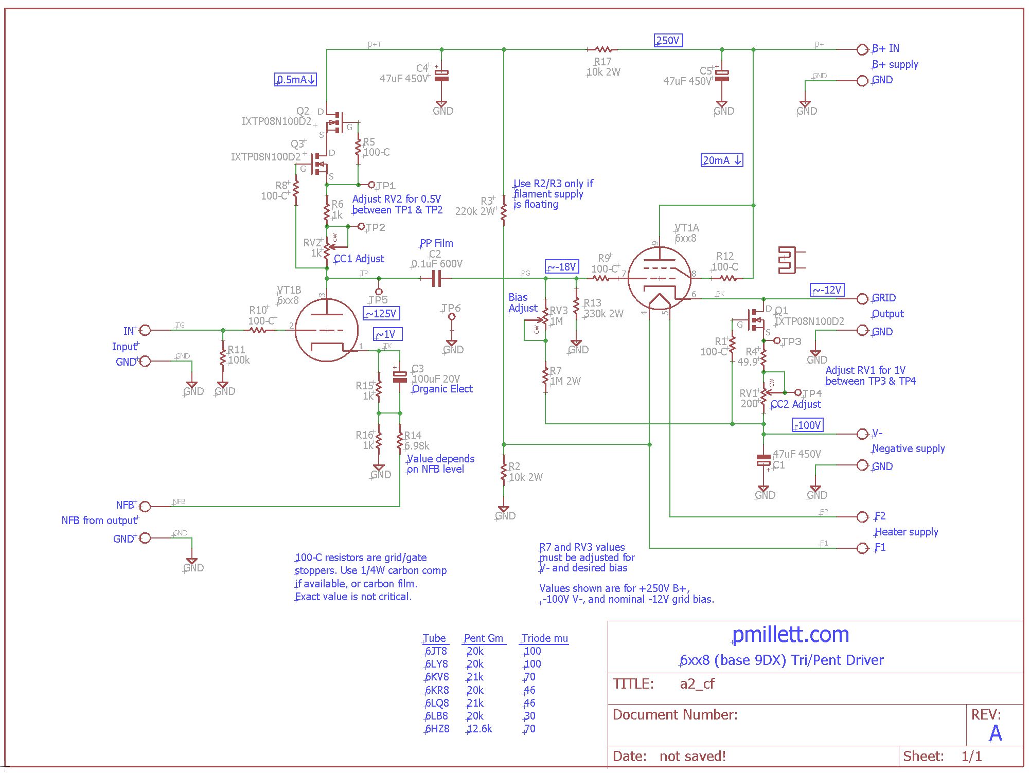
Voltages and currents are shown for the implementation I used for the VT-62 amp. Note that the power tube bias is set with a voltage divider on the cathode follower grid. With the cathode follower CCS set at 20mA, the cathode will be about 6V lower than the grid. That's why you see the voltage at the output of -12V, and -18V at the pentode grid.
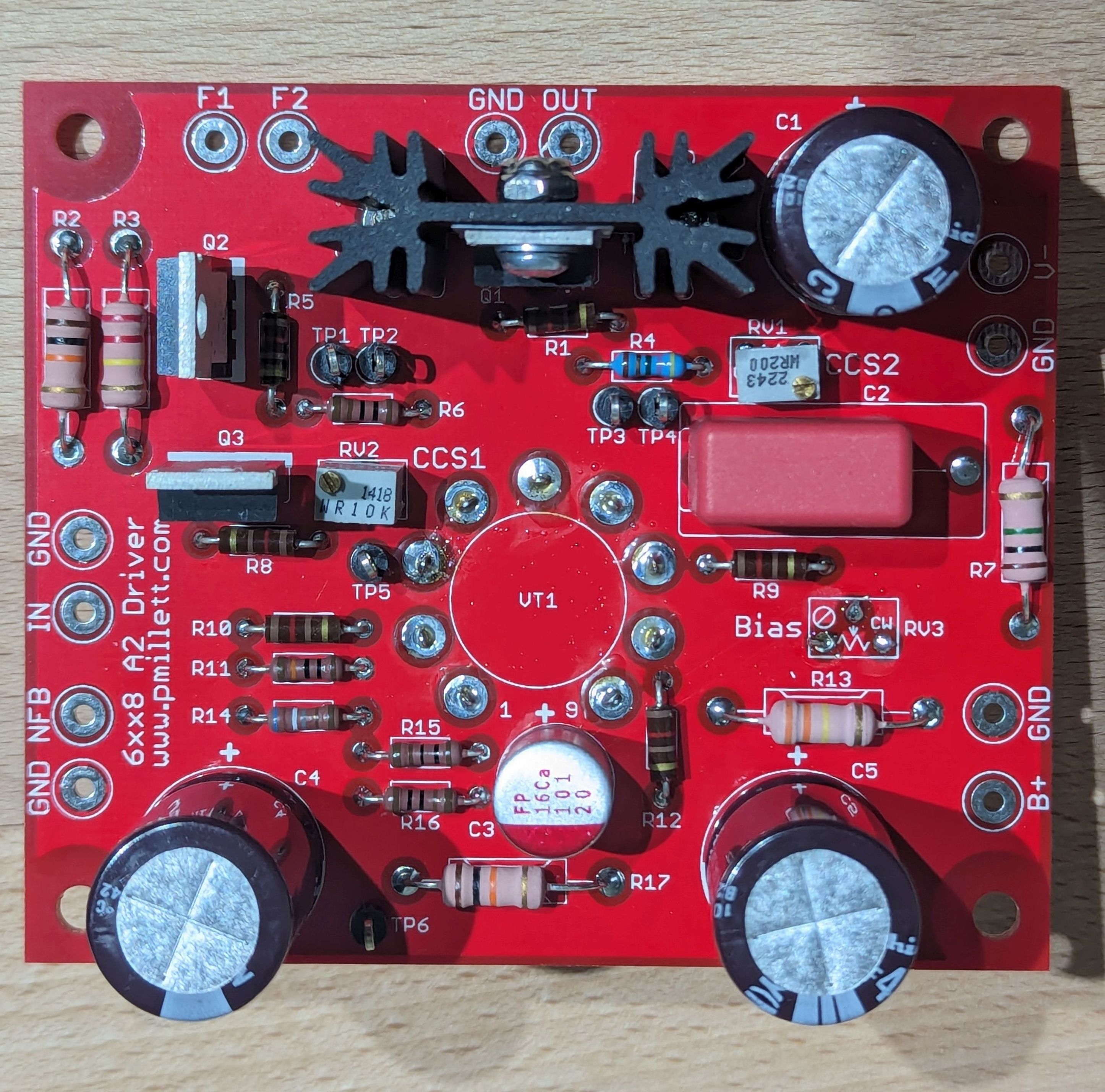
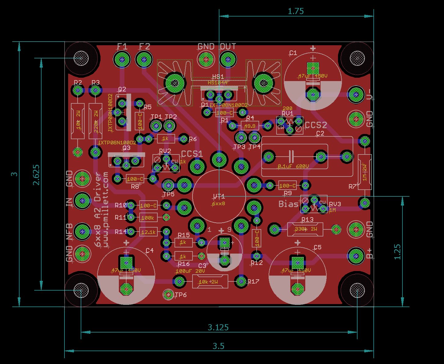
The circuit is contained on a small 3.5" x 3" (sorry for the imperial dimensions, civilized world) PC board with components on one side and the tube on the back side, as is done to poke the tubes out of the top of a chassis. Here is the layout:
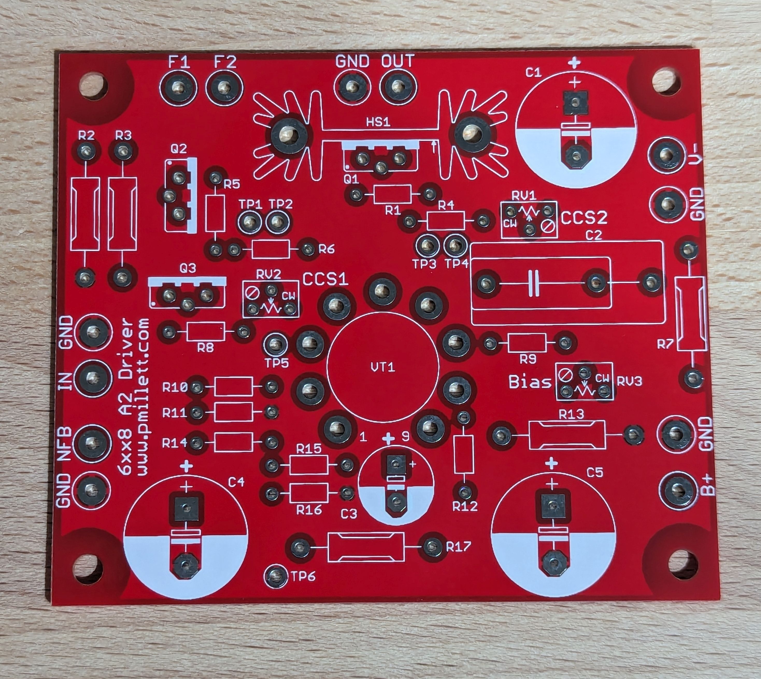
The bare PCB:
You can download a DXF file of the layout to help with chassis design.
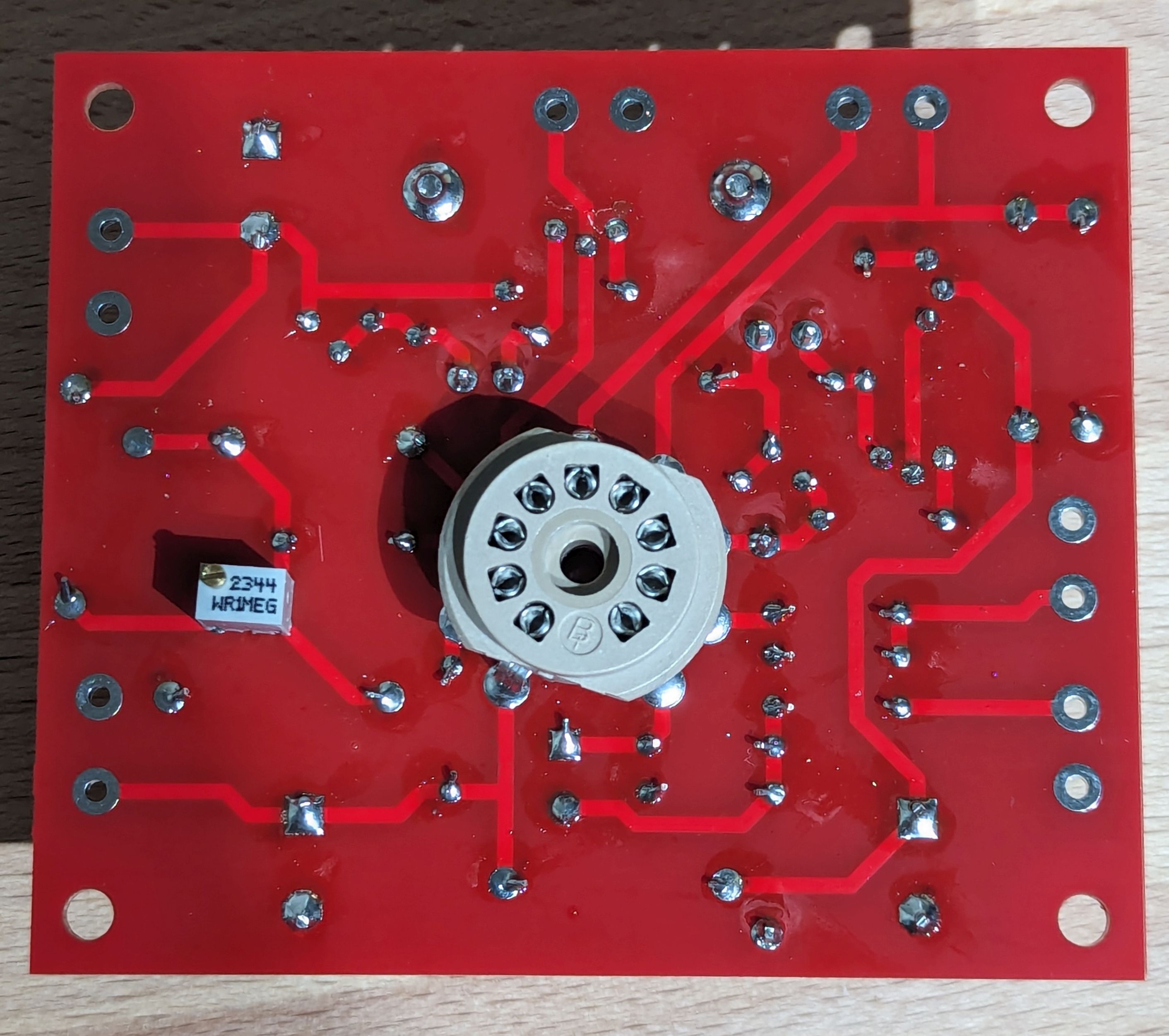
This shows the tube socket on the back. I also placed the bias pot on the back so that I can adjust it from the top through a hole in the chassis:
Here is a bill of materials (BOM or parts list), in .XLS format or PDF format.
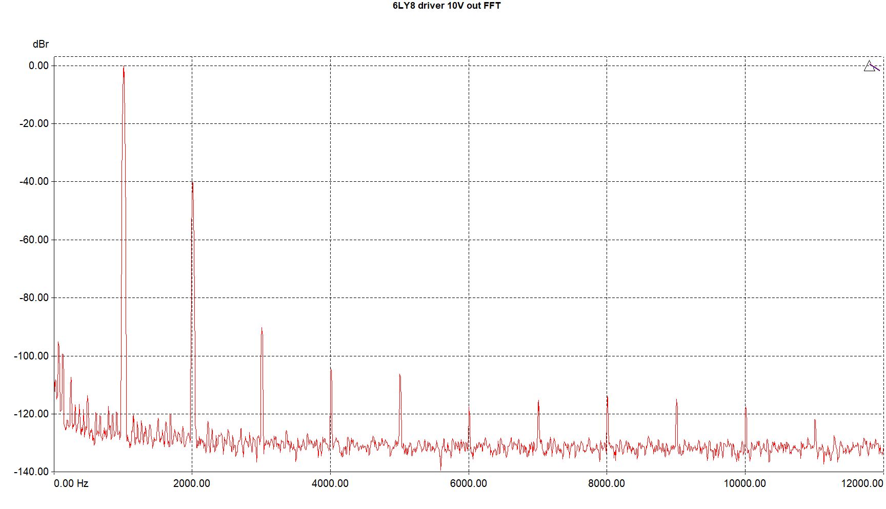
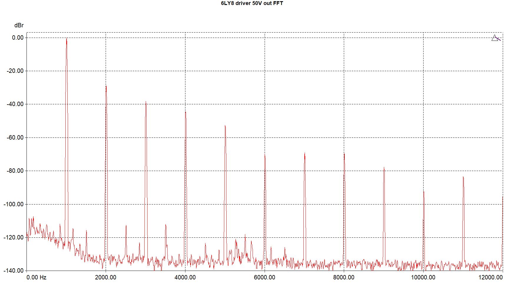
The following measurements are for the circuit configured as shown above. Note that it is not particularly low in distortion, and has a dominant 2nd order harmonic. There are two reasons that this is OK here: one is that this is intended to be used in an amp with significant loop NFB. That's also why it's OK that the first stage is biased with the grid only at about 1V. The second reason (and this is controversial) is that in my experience, at least some 2nd order distortion in the driver will cancel with the 2nd order distortion in the output stage.
With +250V and -100V supplies, the output clips (5% THD) at about 63V RMS (176V peak-to-peak), with 1.2V RMS in. Keep in mind this is open loop - this will be much different when loop NFB is connected.
The open loop gain is about 35dB, or 57 V/V.
At 10V RMS out, THD @ 1kHz is about 1%... at 10V out, about 3.6%.
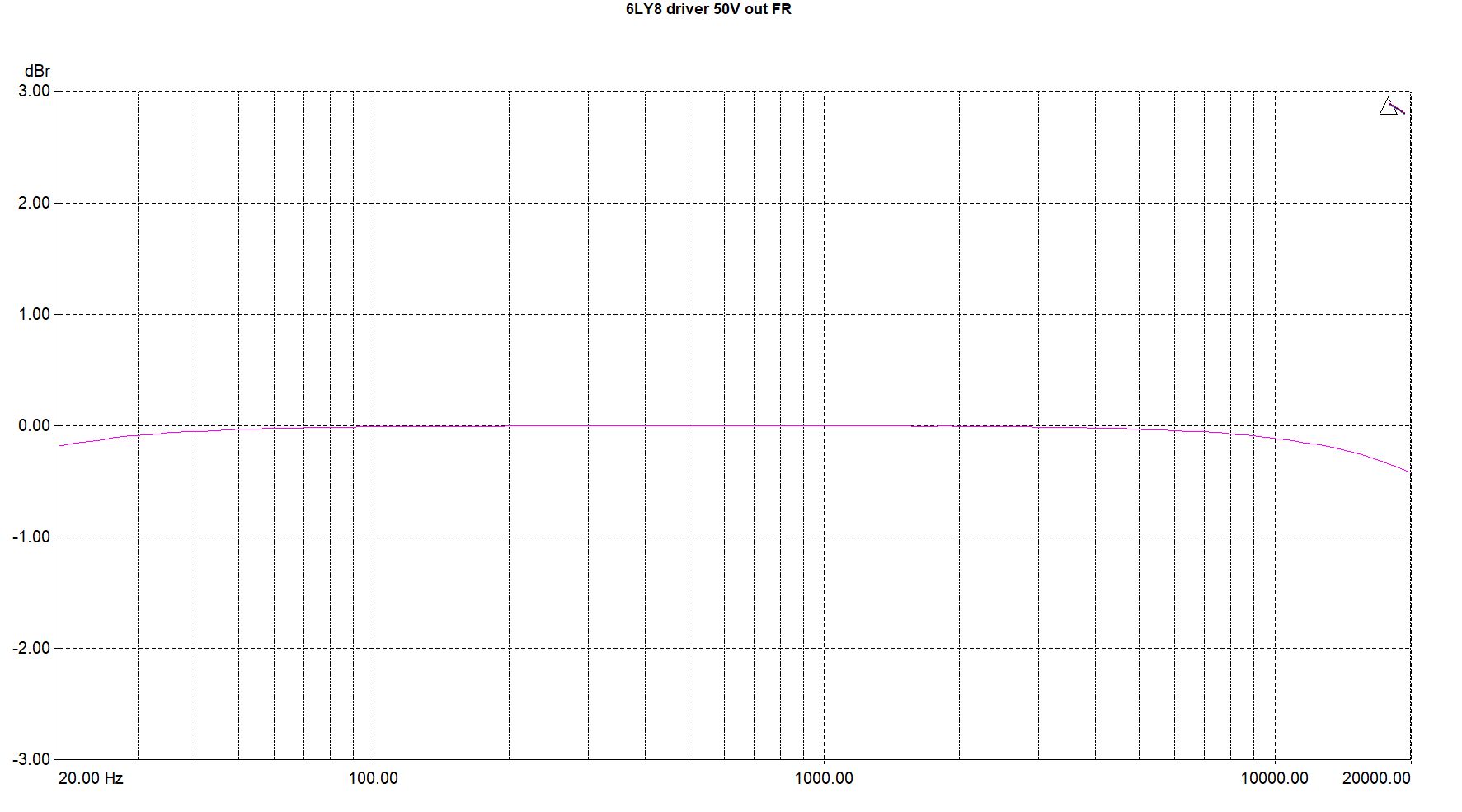
Frequency response is within +0/-0.5dB 20Hz-20kHz:
Here are FFTs of 1kHz, at 10V RMS out, and 50V RMS out: